C26
ENEA Technology
CZTS THIN FILM SOLAR CELLS

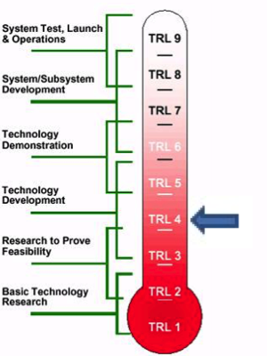
Technology Readiness Level (TRL)
4
Innovations and Benefits
The work is devoted to the development of a semiconductor material based exclusively on abundant and non-toxic elements. This gives clear cost and environmental advantages. The work on the semiconductor Cu2ZnSnS4 (CZTS) started to overcome the production limitations to the CIS (CuInSe2) photovoltaic modules due to the Indium scarcity. CZTS has indeed the same crystallographic structure of the CIS if the Indium is substituted by the Zinc-Tin pair and if the Selenium is substituted by the sulfur: the use of the Sulfur increases the energy gap from 1 eV up to about 1.5 eV. This value of the energy gap is the optimal one for the fabrication of both single junction and tandem photovoltaic devices.
Use
The main goal is the use of CZTS to make the top device in a tandem solar cell where the bottom device is a crystalline silicon solar cell or a thin film solar cell with a low gap. The efficiency of such a device could exceed the 33% limit imposed by thermodynamics to single junction photovoltaic devices.
Applications and ongoing Activities
A complete process for the fabrication of CZTS solar cells on glass has been developed in ENEA and has produced devices with an efficiency nearly to 8%. The further optimization of the process, its extension to the production of CZTS solar cells on silicon substrates and of CZTS/c-Si tandem solar cells is ongoing.
“If you are interested in this technology/service, please send a message to eneaperlinnovazione@enea.it, by specifying the title of the technology/service of your interest, the reason for your request and your contacts or the contacts of a person from your organization/company.
