
C26
ENEA Technology
NANOMACHINING BY FOCUSED ION BEAM
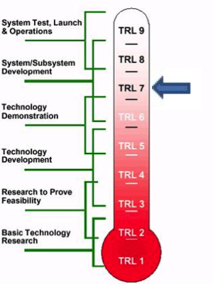
Technology Readiness Level (TRL)
5÷7
Innovations and Benefits
Focused Ion Beam (FIB) is based on direct milling, without photolithographic steps, to modify the surface of any solid material (semiconductors, polymers, metals and insulators), by creating 3D micro/nanometric pattern. By means of finely focused gallium ion beam, FIB can modify and image samples. With the right working conditions, the tool removes selectively any material from surface with a resolution of 10 nanometer, modifying then electrical and physical properties of pristine materials. FIB can deposite the micro/nano pattern of platinum, by means of a organometallic gas injection, on the surface of the sample, by realizing, for example, nanometric electrical contacts. Another peculiarity of FIB is milling very precise cross section (below 100 nm accuracy) of optoelectronic devices for subsequent imaging of inner layers, directly by FIB, which, detecting emitted electrons from samples, provide unique information for its contrast mechanism. FIB is inserted in a more complex apparatus, called Dual Beam, which integrates a SEM microscope, used for further imaging analysis.
Use
Fabrication of metasurfaces on optical fibers for the development of rapid and precise lab-on-fiber for detection of cancer markers, air pollution, toxic contaminants. Milling of nanochannels on two-terminal organic devices for the development of biomolecular sensor devices.
Deposition of platinum nanoelectrodes for hydrogen sensors based on palladium nanowires.
Surface modification on thin fiilm silicon photovoltaic devices to improve light absorption.
Applications and ongoing Activities
Collaboration with Optoelectronic Division - Engineering Department of University of Sannio since 2012 for nanomachining on optical fiber and light trapping optimization in solar cells based on silicon thin film supported by the Italian Ministry of Economic Development in the framework of the Operating Agreement with ENEA for Research on the Electric System; collaboration with Department of Physics of University “Federico II” and CNR-SPIN group of Naples for nanochannel milling in 2 terminal organic devices.
“If you are interested in this technology/service, please send a message to eneaperlinnovazione@enea.it, by specifying the title of the technology/service of your interest, the reason for your request and your contacts or the contacts of a person from your organization/company.