C24
ENEA Technology
RECOVERY OF HIGH-VALUE METALS FROM PRINTED CIRCUIT BOARDS

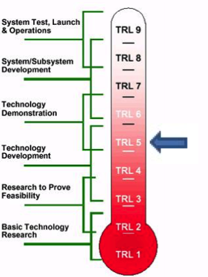
Technology Readiness Level (TRL)
5
Innovations and Benefits
We developed a hydrometallurgical process for the recovery of metals (Au, Ag, Sn, Cu, Pd, Fe and Pb) from printed circuit boards (international patent application PCTIB2014065131 and European Patent Application n. EP 16 713 072.3).
This invention offers a versatile methodology which allows avoiding mechanical pretreatment of PCBs to recover elements with high purity both in metallic form and as inorganic compounds.
The process avoids the use of cyanides for gold recovery and the unit operations –carried out at room temperature– allow reducing energy consumption and operational costs as well as gas emissions.
Compared to the state-of-the art processes, our technology has several advantages:
- PCBs are treated as a whole (i.e. not shredded)
- gold and silver are recovered in the first operational unit
- the outputs are obtained with different purity levels and with different characteristics according to the required specifications.
Use
• Recovery of materials contained in waste PCBs coming from household computers
• Reduction of the amount of waste containing hazardous components (for example heavy metals)
• Possibility to adapt the process to PCBs coming from other types of WEEE (for example smartphones, data transfer systems etc.)
Applications and ongoing Activities
• Lab and pre-pilot tests to verify the recovery yields and the conditions for industrial upscaling.
• Mass balance and air emissions and secondary waste streams assessment, in order to reuse them in the production chain, thus minimizing process costs and reducing the environmental impact.
• Pilot plant engineering
“If you are interested in this technology/service, please send a message to eneaperlinnovazione@enea.it, by specifying the title of the technology/service of your interest, the reason for your request and your contacts or the contacts of a person from your organization/company.
