
M72
ENEA Technology
SYNTHESIS OF NANOSTRUCTURES WITH DIFFERENT MORPHOLOGIES
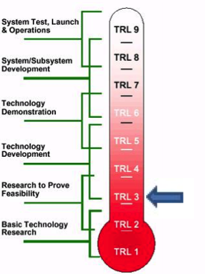
Technology Readiness Level (TRL)
3
Innovations and Benefits
Synthesis of nanostructures with controlled dimensions and morphology. Thin films growth by CVD (Chemical Vapour Deposition), MOCVD and PVD (Physical Vapour Deposition). Sample analysis by electron spectroscopy techniques (XPS, XAES, LEED, EELS e IPES)
The grown nanostructures find applications in energy (storage, PV), environment/biochemistry (sensors) and photonics (QLED).
Use
Nanostructures applications range from energy to electronics and photonics. Important fields are photovoltaics (PV), energy storage, fuel cells, devices and screen (QLED) technology.
Applications and ongoing Activities
Diffuse smart grids, electric traction, renewable sources demand the development of suitable storage systems. Li-ion batteries are important and promising candidates for such applications and the improvement of their charge capacity and the charge/discharge current properties is a crucial issue in order to allow application in these fields. In the framework of "Ricerca Sistema Elettrico" funded by the "Ministero dello Sviluppo Economico", wire-like nanostructures made of Si were synthesized with the aim to improve the anode in Li-ion batteries. Si nanowires were obtained by means of CVD using SiH4 as the precursor gas and Au, Ag and Cu as catalysers. Si nanowires are promising because Si has a 10- times bigger specific capacity than graphite and at the nanoscale the volume expansion due to lithiation does not lead to material pulverization.
“If you are interested in this technology/service, please send a message to eneaperlinnovazione@enea.it, by specifying the title of the technology/service of your interest, the reason for your request and your contacts or the contacts of a person from your organization/company.